14 Angstrom Module Integration
Since May 2023 ipaMS and the Physical & Theoretical Chemistry (PTC) are part of the EU-project 14AMI (14 Angstroms Module Integration) within the HORIZON-KDT-JU-2022 call. Together with 30 internationally renowned partners from the semiconductor sector a total funding of 25 M€ has been approved, with our group being funded with 0.5 M€ over the next three years.
Extreme ultraviolet (EUV) lithography has proven to be a revolutionary technology in the semiconductor industry. It enables the miniaturization of chips with nanometer-scale feature sizes, leading to more powerful semiconductor devices. This is a critical breakthrough in areas such as artificial intelligence, machine learning, mobility, communications, data processing, and computing, just to name a few. EUV lithography uses light with a wavelength of 13.5 nanometers, which is much shorter than the light used in traditional lithography. This allows for the creation of smaller, more precise features on chips, however, demands for unprecedent technological challenges as well.
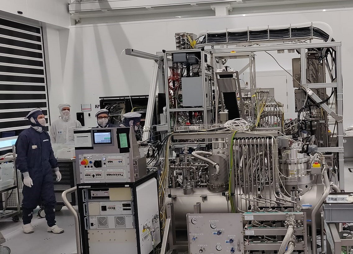
In several different workpackages 14AMI tackles those challenges for the next generation EUV-scanner systems. Our group is involved in the lifetime of the highly sensitive optical elements. Impurities that are produced by the EUV induced plasma degrade the mirror surfaces and essentially reduce their reflectivity, thus less 13.5 nm light is available for the lithography process. With our sensitive mass spectrometric equipment we measure on-site at different EUV sources ultra-trace compounds present in those systems.